In the field of energy transformation, the share of renewable energies continues to grow and gives hope to fight against global warming. In the global electricity mix we have: 15% for hydropower, and 14.5% for other renewables, according to 2022 figures. Among renewable energies, photovoltaic (PV) solar energy is the most promising with very high record yields of around 29% theoretically, 27.3% experimentally for record-breaking PV solar cells in the laboratory and 22% in industrial production for a solar panel. The selenide, gallium, indium and copper (CIGS) sector is very promising, one of its major advantages coming that the fact the quaternary alloy Cu(In,Ga)Se2 is a material with an adjustable bandgap (Eg). The freely available and highly stable one-dimensional solar cell capacities simulation software, is the tool used for the simulation. Digital simulation is an essential tool because it makes it possible to predict the behavior of the solar device and to be able to estimate its performances. The study of effects of the thickness (WCIGS) and the gap of the CIGS absorber with a cadmium sulfide buffer layer of 30 nm shows that current-voltage density characteristic is enormously affected for WCIGS ≤1000 nm. We therefore note a significant decrease in the values of the short-circuit current density (JSC) and the open-circuit voltage (VOC) when WCIGS decreases. These results are explained by a significant reduction in the quantity of incident photons absorbed and an increase in the recombination rate of the charge carriers photogenerated in the absorber. VOC increases and JSC decreases with the increasing of the absorber gap, the increase in VOC is therefore linked to a significant reduction in the recombination rate at the CIGS/Mo interface and inside the space charge region. The maximum efficiency is 26.33% for Eg = 1.45 eV and WCIGS = 3000 nm.
| Published in | American Journal of Energy Engineering (Volume 14, Issue 1) |
| DOI | 10.11648/j.ajee.20261401.11 |
| Page(s) | 1-8 |
| Creative Commons |
This is an Open Access article, distributed under the terms of the Creative Commons Attribution 4.0 International License (http://creativecommons.org/licenses/by/4.0/), which permits unrestricted use, distribution and reproduction in any medium or format, provided the original work is properly cited. |
| Copyright |
Copyright © The Author(s), 2026. Published by Science Publishing Group |
Numerical Simulation, Quaternary Thin Film Solar, Cu(In, Ga)Se2 Absorber, Thickness, Bandgap, Electricals Parameters
 (1)
(1) Contacts properties | ||
|---|---|---|
Parameters | Right | left |
|
|
|
|
|
|
|
|
|
Reflectivity |
|
|
p-CIGS | n-CdS | n-OVC | i-ZnO | n-ZnO | |
|---|---|---|---|---|---|
Layers properties | |||||
W (nm) | 1000 | 30 | 1 | 80 | 100 |
Eg (eV) | 1.2 | 2.4 | 1.45 | 3.4 | 3.3 |
| 4.5 | 4.45 | 4.5 | 4.55 | 4.45 |
ɛ/ɛ0 | 13.6 | 10 | 13 | 9 | 9 |
Nc (cm-3) | 2.2*1018 | 2.2*1018 | 2*1018 | 4*1018 | 2.2*1018 |
Nv (cm-3) | 1.8*1019 | 1.8*1019 | 2*1019 | 3*1019 | 1.8*1019 |
ѵe (cm/s) | 5*106 | 107 | 5*105 | 107 | 107 |
ѵh (cm/s) | 5*106 | 107 | 5*105 | 107 | 107 |
µe (cm2/Vs) | 102 | 102 | 1 | 50 | 102 |
µh (cm2/Vs) | 25 | 25 | 1 | 20 | 25 |
Na (cm-3) | 2.5*1016 (a) | - | 1013 (a) | - | - |
Nd (cm-3) | - | 2.5*1016 (d) | - | 5*1017 (d) | 1018 (d) |
| 0.35 | -0.3 | - | - | - |
Bulk defect properties | |||||
σe (cm2) | 6.1*10-14 | 10-17 | - | - | 10-14 |
σh (cm2) | 10-14 | 10-13 | - | - | 10-15 |
NAG, NAG (cm-3) | 3*1014 (d) | 1017 (a) | - | - | 1013 (a) |
EA, ED (eV) | 0.6 | 1.2 | - | - | 1.65 |
WG (eV) | 0.1 | 0.1 | - | - | 0.1 |
 (2)
(2) CdS | Cadmium Sulfide |
CdTe | Cadmium Telluride |
CIGS | Copper Indium Gallium Selenide |
CIS | Copper Indium Selenide |
CZTS | Copper Zinc Tin Sulfur |
Eg | Bandgap Energy |
GaAs | Gallium Arsenide |
Na2O2 | Soda Glass |
OTC | Oxide Transparent Conductive |
PV | Photovoltaic |
SCAPS-1D | One-dimensional Solar Cell Capacities Simulation |
ZnO | Zinc Oxide |
| [1] | Kébré, M. B., Zougmoré, F., Oubda, D., S., Ouédraogo, & Koalaga, Z. 2012. Influence of the thickness of the buffer layer and the temperature on the properties of a photocell in thin layers based on CIGS. In: CIFEM2012. |
| [2] | Fabrication and characterization of CuInGaSe2 films by cathode sputtering Study of defects by charge-based deep trap spectroscopy. Ph.D. thesis, University of Nantes. |
| [3] |
Planet energies. Renewable energies.
www.planete-energies.com (17/01/2026). |
| [4] | Science and the Future; Sustainable Development. Photovoltaics: the subtle revolution of solar cells. |
| [5] |
LONGI. Sets a new world record for conversion efficiency of 34.85% for 2025 silicon-perovskite tandem solar cells.
http://www.plein-soleil.info (20/12/2025). |
| [6] |
Philippe P. 2013 A new record of 44.7% for photovoltaics! The new factory
https://www.usinenouvelle.com (20/12/2025). |
| [7] | Jie, Z., Bo, L., Shuying, C., &Weibo, Z. 2013. Effects of Sulfurization Temperature on Properties of CZTS Films by Vacuum Evaporation and Sulfurization Method. Hindawi Publishing Corporation International Journal of Photoenergy, 2013, |
| [8] | Oubda, D., Diasso, A., Ouédraogo, B., Kabré, S., Kébré, M. B., Ouédraogo, S., Traoré, B., Zongo, A., Sankara, I., Sawadogo, P., Barry, A., Sawadogo, B. and Zougmoré, F. (2025) Numerical Simulation of the Dominate Recombination Mechanism in the Chalcopyrite Cu(In,Ga)Se2 Thin Film Solar Cell. Open Journal of Applied Sciences, 15, 3663-3672. |
| [9] | Lundberg, O. 2003. Band gap Profiling and high speed deposition of Gu(In,Ga)Se2 for thin film solar cells. Ph.D. thesis, Uppsala. |
| [10] | Jiyon, S., Sheng, S., Li, C. H., Huang, O. D., Crisalle, T., & Anderson, J. 2004. Device modeling and simulation of the performance of Cu(In1-x,Gax)Se2 solar cells. Solid-State Electronics, 48 (2004), 7379. |
| [11] | Gloeckler, M, Sites, J. R., &. 2005. Band-gap grading in Cu(In,Ga)Se2 solar cells. Journal of Physics and Chemistry of Solids 66 (2005) 18911894, 66 (2005), 18911894. |
| [12] | Gloeckler, M. 2005. Device physics of Cu(In,Ga)Se2 thin-film solar cells. Ph.D. thesis, Colorado State University. |
| [13] | Ouédraogo, S. 2016. Numerical modeling of a thin film solar cell based on CIGS. Ph.D. thesis, Ouaga I University Professor J. K. Zerbo, Ouagadougou. |
| [14] | Oubda, D. 2018. “Characterisation of Thin Film Solar Cell as Function of Buffer Layer Nature.” Doctoral thesis, University of Professor Joseph KI-ZERBO, Ouagadougou. |
| [15] | Ouedraogo, S., Kebre, M. B., Ngoupo, A. T., Oubda, D. and Zougmore, F. (2020) Comprehensive Analysis of CuIn1−xGaxSe2 Based Solar Cells with Zn1−yMgyO Buffer Layer. Materials Sciences and Applications, 11, 880-892. |
| [16] | Kanevce, A. 2007. Anticipated performance of Cu(In,Ga)Se2 solar cells in the thin film limit. Ph.D. thesis, Colorado State University. |
| [17] | Ouedraogo, S., Kebre, M. B., Ngoupo, A. T., Oubda, D., Zougmore, F. and Ndjaka, J.-M. (2020) Required CIGS and CIGS/Mo Interface Properties for High-Efficiency Cu(In,Ga)Se2 Based Solar Cells. Advances in Materials Physics and Chemistry, 10, 151-166. |
| [18] | Dullweber, T., Hanna, G., Shams-Kolahi., G., Schwartzlander, A., Contreras, M. A., Noufi, R., & Schock, H. W. 2000. Study of the effect of gallium grading in Cu(In,Ga)Se2. Thin Solid Films, 361-362, 478–481. |
| [19] | Oubda, D., Kebre, M. B., Zougmoré, F., Njomo, D., and Ouattara, F. 2015. “Numerical Simulation of Cu(In,Ga)Se2 Solar Cells Performances.” Journal of Energy and Power Engineering 9: 1047-55. |
| [20] | Oubda, D., Kebre, M. B., Ouédraogo, S., Zougmoré, F., Ouattara, F., and Koalga, Z. 2018. “Numerical Characterization of Cu(In,Ga)Se2 Solar Cells Using Capacitance-Voltage and Capacitance-Frequency Characteristics.” International Journal of Progressive Sciences and Technologies (IJPSAT) 6 (2): 262-7. |
| [21] | Zongo, A., Oubda, D., Ouédraogo, S., Kébré, M. B., Diasso, A., Sankara, I., Traore, B., Zougmoré, F., Koalga, Z. and Ouattara, F. (2021) Optimization of Mo/Cu(In, Ga)Se2/CdS/ZnO Hetero-Junction Solar Cell Performance by Numerical Simulation with SCAPS-1D. Journal of Materials Science and Engineering B, 11, 156-167. |
| [22] |
Niemegeers, A., Burgelman, M., Herberholz, R., Rau, U., Hariskos, D., & Schock, H.-W. 1998. Model for electronic transport in Cu(In,Ga)Se2 Solar Cells. PROGRESS IN PHOTOVOLTAICS 6, 407–421.
https://doi.org/10.1002/(SICI)1099-159X(199811/12)6:6<407::AID-PIP230>3.0.CO;2-U |
| [23] | Khelifi, S., & Belghachi, A. 2004. The Role of the Window Layer in Dune Performance GaAs Solar Cell. Rev. Energ. Ren., Vol. 7 (2004), 13–21. |
| [24] | Niemergeers, A., & Burgelman, M. 1997. Effects of the Au/CdTe back contact on IV and CV characteristics of Au/CdTe/CdS/TCO solar cells. J. Appl. Phys., 81, No. 6, 2881–2886. |
| [25] | Burgelman, M., Nollet, P., & Degrave, S. 2000. Modelling polycrystalline semiconductor solar cells. Thin Solid Film, 361-362(2000); 527-532: |
| [26] | Yiming, L., Yun, S., & Angus, R. 2011. A new simulation software of solar cells-wxAMPS. Solar Energy Materials and Solar Cells, (2011), p. 1–5. |
| [27] | Sawadogo B. 2025 Analysis of the influence of the absorber layer and temperature on amorphous silicon-based PV solar cell. Master's thesis, Joseph Ki-Zerbo University. |
| [28] | Oubda, D., Kebre, M. B., Ouedraogo, S., Diasso, A., Zougmore, F., Koalga, Z. and Ouattara, F. (2022) High Performance for Cu(In,Ga)Se2 Quaternary System-Based Solar Cells with Alternative Buffer Layers. Advances in Materials Physics and Chemistry, 12, 207-219. |
| [29] | Ouédraogo S., Traoré B., Kébré B. M., Oubda D., Zongo A., Sankara I. and Zougmoré F. (2020). Performance Enhancement Strategy of Ultra-Thin CIGS Solar Cells. American Journal of Applied Sciences, 2020, Volume 17, pp. 246 255. |
| [30] | Arturo, Morales-Acevedo. 2010. A Simple Model of Graded Band-Gap CuInGaSe2 Solar Cells. Energy Procedia 2 (2010) 169176, 2 (2010), 169176. |
| [31] | Chelouche, salim. 2012. Properties of ZnO: Al optical winows for CIGS-based thin-film solar cells. M. Phil. thesis Ferhat Abbas Setif University. |
APA Style
Oubda, D., Kabre, S., Diasso, A., Ouedraogo, B., Kebre, M. B., et al. (2026). Simulation of the Effects of the Thickness and the Bandgap of the Absorber on the Performance of the Quaternary Thin Film Solar Cell Based on Cu(In,Ga)Se2. American Journal of Energy Engineering, 14(1), 1-8. https://doi.org/10.11648/j.ajee.20261401.11
ACS Style
Oubda, D.; Kabre, S.; Diasso, A.; Ouedraogo, B.; Kebre, M. B., et al. Simulation of the Effects of the Thickness and the Bandgap of the Absorber on the Performance of the Quaternary Thin Film Solar Cell Based on Cu(In,Ga)Se2. Am. J. Energy Eng. 2026, 14(1), 1-8. doi: 10.11648/j.ajee.20261401.11
AMA Style
Oubda D, Kabre S, Diasso A, Ouedraogo B, Kebre MB, et al. Simulation of the Effects of the Thickness and the Bandgap of the Absorber on the Performance of the Quaternary Thin Film Solar Cell Based on Cu(In,Ga)Se2. Am J Energy Eng. 2026;14(1):1-8. doi: 10.11648/j.ajee.20261401.11
@article{10.11648/j.ajee.20261401.11,
  author = {Daouda Oubda and Sayouba Kabre and Alain Diasso and Boureima Ouedraogo and Marcel Bawindsom Kebre and Soumaila Ouedraogo and Boureima Traore Issaka Sankara and Adama Zongo and Amidou Barry and Boureima Sawadogo and Pindewinde Sawadogo and François Zougmore},
  title = {Simulation of the Effects of the Thickness and the Bandgap of the Absorber on the Performance of the Quaternary Thin Film Solar Cell Based on Cu(In,Ga)Se2},
  journal = {American Journal of Energy Engineering},
  volume = {14},
  number = {1},
  pages = {1-8},
  doi = {10.11648/j.ajee.20261401.11},
  url = {https://doi.org/10.11648/j.ajee.20261401.11},
  eprint = {https://article.sciencepublishinggroup.com/pdf/10.11648.j.ajee.20261401.11},
  abstract = {In the field of energy transformation, the share of renewable energies continues to grow and gives hope to fight against global warming. In the global electricity mix we have: 15% for hydropower, and 14.5% for other renewables, according to 2022 figures. Among renewable energies, photovoltaic (PV) solar energy is the most promising with very high record yields of around 29% theoretically, 27.3% experimentally for record-breaking PV solar cells in the laboratory and 22% in industrial production for a solar panel. The selenide, gallium, indium and copper (CIGS) sector is very promising, one of its major advantages coming that the fact the quaternary alloy Cu(In,Ga)Se2 is a material with an adjustable bandgap (Eg). The freely available and highly stable one-dimensional solar cell capacities simulation software, is the tool used for the simulation. Digital simulation is an essential tool because it makes it possible to predict the behavior of the solar device and to be able to estimate its performances. The study of effects of the thickness (WCIGS) and the gap of the CIGS absorber with a cadmium sulfide buffer layer of 30 nm shows that current-voltage density characteristic is enormously affected for WCIGS ≤1000 nm. We therefore note a significant decrease in the values of the short-circuit current density (JSC) and the open-circuit voltage (VOC) when WCIGS decreases. These results are explained by a significant reduction in the quantity of incident photons absorbed and an increase in the recombination rate of the charge carriers photogenerated in the absorber. VOC increases and JSC decreases with the increasing of the absorber gap, the increase in VOC is therefore linked to a significant reduction in the recombination rate at the CIGS/Mo interface and inside the space charge region. The maximum efficiency is 26.33% for Eg = 1.45 eV and WCIGS = 3000 nm.},
 year = {2026}
}
TY  - JOUR
T1  - Simulation of the Effects of the Thickness and the Bandgap of the Absorber on the Performance of the Quaternary Thin Film Solar Cell Based on Cu(In,Ga)Se2
AU  - Daouda Oubda
AU  - Sayouba Kabre
AU  - Alain Diasso
AU  - Boureima Ouedraogo
AU  - Marcel Bawindsom Kebre
AU  - Soumaila Ouedraogo
AU  - Boureima Traore Issaka Sankara
AU  - Adama Zongo
AU  - Amidou Barry
AU  - Boureima Sawadogo
AU  - Pindewinde Sawadogo
AU  - François Zougmore
Y1  - 2026/01/29
PY  - 2026
N1  - https://doi.org/10.11648/j.ajee.20261401.11
DO  - 10.11648/j.ajee.20261401.11
T2  - American Journal of Energy Engineering
JF  - American Journal of Energy Engineering
JO  - American Journal of Energy Engineering
SP  - 1
EP  - 8
PB  - Science Publishing Group
SN  - 2329-163X
UR  - https://doi.org/10.11648/j.ajee.20261401.11
AB  - In the field of energy transformation, the share of renewable energies continues to grow and gives hope to fight against global warming. In the global electricity mix we have: 15% for hydropower, and 14.5% for other renewables, according to 2022 figures. Among renewable energies, photovoltaic (PV) solar energy is the most promising with very high record yields of around 29% theoretically, 27.3% experimentally for record-breaking PV solar cells in the laboratory and 22% in industrial production for a solar panel. The selenide, gallium, indium and copper (CIGS) sector is very promising, one of its major advantages coming that the fact the quaternary alloy Cu(In,Ga)Se2 is a material with an adjustable bandgap (Eg). The freely available and highly stable one-dimensional solar cell capacities simulation software, is the tool used for the simulation. Digital simulation is an essential tool because it makes it possible to predict the behavior of the solar device and to be able to estimate its performances. The study of effects of the thickness (WCIGS) and the gap of the CIGS absorber with a cadmium sulfide buffer layer of 30 nm shows that current-voltage density characteristic is enormously affected for WCIGS ≤1000 nm. We therefore note a significant decrease in the values of the short-circuit current density (JSC) and the open-circuit voltage (VOC) when WCIGS decreases. These results are explained by a significant reduction in the quantity of incident photons absorbed and an increase in the recombination rate of the charge carriers photogenerated in the absorber. VOC increases and JSC decreases with the increasing of the absorber gap, the increase in VOC is therefore linked to a significant reduction in the recombination rate at the CIGS/Mo interface and inside the space charge region. The maximum efficiency is 26.33% for Eg = 1.45 eV and WCIGS = 3000 nm.
VL  - 14
IS  - 1
ER  -
Doctoral School of Sciences and Technologies, Joseph KI-ZERBO University, Ouagadougou, Burkina Faso
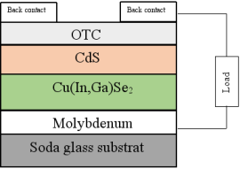
Figure 1. Structure of CIGS-based solar cell.
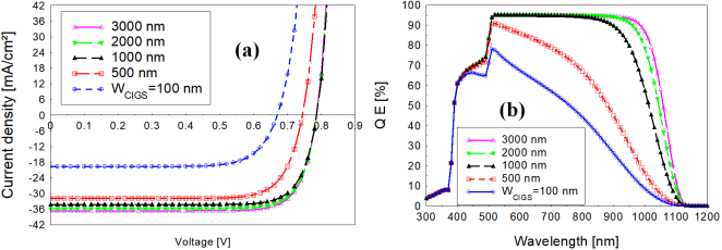
Figure 2. (a) J-V characteristics, (b) quantum efficiency as a function of CIGS thickness.
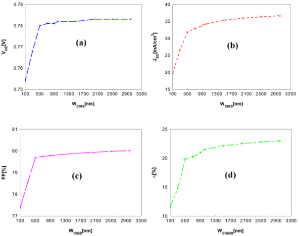
Figure 3. Electrical parameters as function on the thickness of the CIGS.
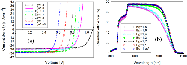
Figure 4. (a) J-V characteristic, (b) quantum efficiency as a function of the bandgap of the CIGS absorber.
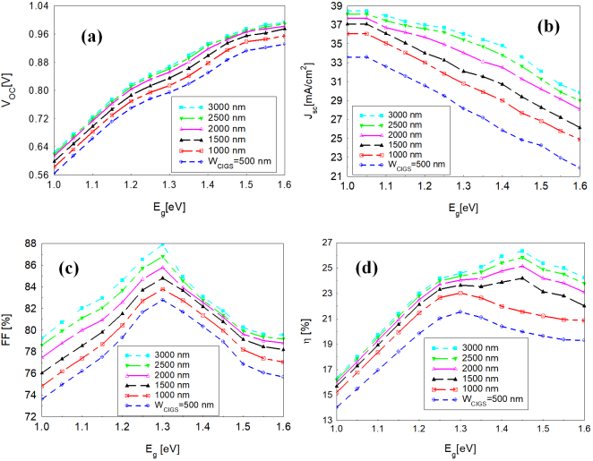
Figure 5. Electrical parameters as a function of the bandgap and for different thicknesses of the absorber.
Table 1. Base parameters of CIGS cell properties. ![]() —barrier height (
—barrier height (![]() ,
, ![]() ), Se and Sh—surface recombination velocity electron and hole, W —layer width,
), Se and Sh—surface recombination velocity electron and hole, W —layer width, ![]() —dielectric constant,
—dielectric constant, ![]() —mobility, Doping (electron/hole density), Eg—band gap energy, NC and NV —effective density of states,
—mobility, Doping (electron/hole density), Eg—band gap energy, NC and NV —effective density of states, ![]() —conduction band offset, NAG —acceptor-like defect density, NDG —donor-like defect density, EA and ED —peak energy in,
—conduction band offset, NAG —acceptor-like defect density, NDG —donor-like defect density, EA and ED —peak energy in, ![]() and,
and, ![]() —capture cross section electrons and holes,
—capture cross section electrons and holes, ![]() —electron affinity,
—electron affinity, ![]() —thermal velocity, WG —characteristic energy, Na, Nd —shallow uniform acceptor and donor [13-15, 17, 19, 21, 28, 29].
—thermal velocity, WG —characteristic energy, Na, Nd —shallow uniform acceptor and donor [13-15, 17, 19, 21, 28, 29].
Information


 (eV)
(eV) (eV)
(eV)